
Modern electronics would not be what it is without PCB layout design. All the devices that you handle in your everyday life rely on these complex blueprints. The printed circuit boards drive the technological world of smartphones and even spaceships.
This handy reference book discloses the fundamental concepts of PCB layout design. You will learn the essential procedures, industry pitfalls, and commercial practices necessary to distinguish between casual shaving boards and professional-quality surfaces.
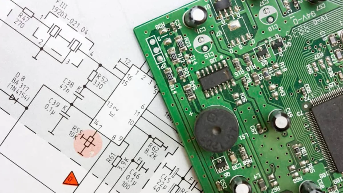
What is PCB Layout Design?
It defines the signal behavior among parts. On the layout, the roadmap, which is the physical means of connecting the electricity, occurs. It is like architectural planning of technology. Each of the resistors, capacitors, and integrated circuits requires its ideal place. Electrical performance has to be balanced against the manufacturing limitations by the designer. Bad design can lead to equipment failures, electromagnetic disturbances, and delays. Professional layouts provided the guarantees of scarcely affected work under different circumstances.
The importance of PCB Layout Design.
This is the key to the success of your products through PCB board layout design. Several crucial aspects necessitate doing this step:
Signal Integrity Protection
Some of the problems that are caused by poor layouts are noise, crosstalk, and deterioration in signals. Pro designs have clean signal pathways.
Thermal Management
Com parts are hot when in use. Overheating is avoided by placing the strategies. Thermal planning is necessary to ensure longer device life and high reliability.
Cost Control
Optimised arrangements minimise board area and layers. Intelligent designs reduce the use of materials at a minimal cost. Production cost delay is avoided by the manufacturing-friendly layouts.
Regulatory Compliance
Industry-standard layouts are professional. The EMI compliance is a shield against electromagnetic interference. Relevant clearance and creepage distances are needed in safety certification.
Major Elements in PCB Print Design
All parts have certain purposes:
Resistors
These elements regulate current. Wise resort disposition guards against the possibilities of component burnt-out in an overcurrent instance.
Capacitors
Capacitors can hold and give electrical energy. They remove noise in the power supply and regulate voltages.
Integrated Circuits
ICs are complicated to perform in small packages. ICs with high-pin-count need attention in routing to achieve optimum performance.
Conductive Traces
Signals are carried between components on copper. Current-carrying capacity is impacted by trace width. Signal integrity problems are avoided by good trace routing.
PCB Layout Designing Process
There is a systematic process for PCB layout professionally.
Schematic Creation
The scheme is initiated by schematic capture. Circuit versatility is described symbolically by engineers. This outline assists in the planning of the physical layout.
The development of a component library.
A proper component footprint is needed. Verified footprints are employed in professional designs to avoid assembly problems.
Definition Of Board Outline
Size constraints are mechanically based. The placement of connectors tends to predetermine board outline parameters.
Stack-up Planning
Signal routing options have an effect on the number of layers. Stack-up design is a compromise between the considerations of electrical needs and cost. Choice of trace geometry is based on impedance calculations.
Component Placement
Key items are prioritized.
Signal Routing
Trace routing is the linking of components based on the requirements of the scheme. The fast signal requires special methods of routing. Current capacity traces needed in power distribution are wide.
Critical Design Rules for PCB Layout
Layout verification is checked with automated tools. DRC identifies violations of spacing and problems in the manufacturing. All the electrical and physical rule checks are implemented in professionally designed layouts.
- PCB Layout Critical Design Rules
- Trace Width Standard
- Spacing Requirements
- Through Design Guidelines
- Component Orientation
Common PCB Layout Design Challenges
Even experienced designers face significant challenges. Understanding these issues helps prevent costly mistakes:
- Signal Integrity Issues
- Thermal Management Problems
- Electromagnetic Interference
- Manufacturing Constraints
Professional PCB Design Tools
Modern PCB layout services require sophisticated software tools. Leading platforms include:
- Altium Designer
- Cadence Allegro
- KiCad
The Future of PCB Layout Design
New layout issues are propelled by the evolution of technology. Several trends influence the industry:
Miniaturization Demands
Apparatus keeps shrinking and gaining new applications. High-density interconnect (HDI) technology can offer compact designs. New-fangled packaging methods favor internalization of components.
Higher Frequencies
Pushing frequencies to higher levels isa wireless application. The layout of designs meant to work at millimeter wavelengths is much more specialised. RF competence increasingly has value.
Integration of Artificial Intelligence
Routing efficiency enhances the use of machine learning algorithms. More problems are detected with automated design verification.
Conclusion
The key to success is extensive knowledge of electrical, manufacturing, and the use of design tools. The field also requires proper education since technology is updated. The art and science of PCB layout design is a profession. It turns the most abstract ideas into real things that fuel our modern world. Every trace via and even component placement decision impacts the performance, reliability, and cost of the final product.
Appropriate design of PCB layout is worth the investment in the entire product lifecycle. Properly engineered boards are consistent, regulatory-compliant, and efficiently produced. The foundation ensures product success in competitive markets . Your knowledge in PCB layout design turns out to be the gateway to your new skillfulness through innovative ideas that lead to successful products that determine our technical future.