
In modern electronics manufacturing, SMT PCB assembly has revolutionized the way components are placed and soldered onto printed circuit boards. The increasing complexity and miniaturization of electronic devices demand not only precision in assembly but also rigorous quality control (QC) processes to ensure reliable performance. Key technologies such as Solder Paste Inspection (SPI), Automatic Optical Inspection (AOI), and other advanced testing methods play a vital role in maintaining the highest standards in SMT manufacturing.
Why Quality Control Is Critical in SMT PCB Assembly
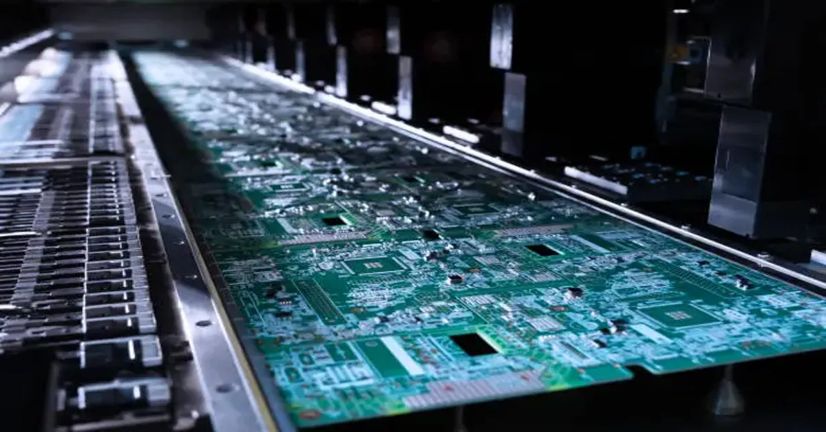
The SMT process involves multiple steps, from stencil printing and pick-and-place to reflow soldering and final inspection. Even minor defects in solder joints, component alignment, or board cleanliness can lead to serious functional issues in the final product.
Quality control ensures:
- Reduced defect rates and rework costs
- Enhanced reliability of electronic devices
- Compliance with industry standards such as IPC-A-610
- Customer satisfaction through consistent product performance
In high-volume production, defects that go undetected early can result in costly recalls and damaged brand reputation.
Solder Paste Inspection (SPI)
Solder paste printing is the first step in SMT assembly, and its quality directly affects the entire process. SPI is an automated process that uses 3D scanning technology to measure the volume, height, and alignment of solder paste deposits on each PCB pad.
Key benefits of SPI include:
- Detects insufficient or excessive solder paste
- Ensures accurate alignment of solder paste with pads
- Provides real-time feedback to the printing machine for correction
By identifying solder paste issues immediately, SPI prevents problems such as solder bridges or open joints from progressing further down the line.
Automatic Optical Inspection (AOI)
AOI is one of the most widely used QC tools in SMT PCB assembly. It uses high-resolution cameras and image processing software to inspect PCBs after soldering.
AOI checks for:
- Incorrect or missing components
- Misaligned or tilted parts
- Poor solder joints, such as cold solder or insufficient wetting
- Polarity errors in components like diodes or electrolytic capacitors
Modern AOI systems employ both 2D and 3D imaging to detect subtle defects. They can be placed at multiple stages—post-placement, pre-reflow, and post-reflow—for maximum efficiency.
In-Circuit Testing (ICT)
ICT is another critical step for quality control in electronics manufacturing. It uses electrical probes to test the continuity, resistance, capacitance, and signal integrity of the assembled PCB.
ICT advantages include:
- Identifies open circuits, shorts, and incorrect component values
- Tests functionality of active components like ICs
- Provides data for process improvement
While ICT requires a custom test fixture, it is highly effective for large production runs where consistent quality is essential.
X-Ray Inspection
X-ray inspection is particularly important for detecting defects in hidden solder joints, such as those under Ball Grid Array (BGA) packages. Optical inspection cannot see through components, making X-ray technology indispensable.
Common issues found by X-ray include:
- Voids in solder joints
- Head-in-pillow defects in BGAs
- Bridging between hidden pads
By ensuring the integrity of hidden solder connections, X-ray inspection greatly improves the reliability of high-density boards.
Functional Testing (FCT)
Functional testing verifies that the assembled PCB performs as intended in its actual application environment. This may involve running the board in a simulated product or using software-based testing protocols.
FCT ensures:
- Power-up and signal flow work correctly
- Firmware or software integrates smoothly
- Performance matches customer requirements
Functional testing is often the final step before boards are shipped to customers.
Integrating Quality Control into the SMT Process
For the best results, quality control should be implemented at multiple points throughout the SMT PCB assembly process, not just at the end. A typical sequence might look like this:
- SPI after solder paste printing
- AOI after component placement
- AOI/X-ray after reflow soldering
- ICT/FCT before final packaging
This layered approach ensures that defects are caught early, reducing waste and improving overall production efficiency.
Conclusion
In today’s competitive electronics market, high-quality SMT PCB assembly is non-negotiable. Technologies such as SPI, AOI, X-ray inspection, ICT, and FCT form a robust quality control ecosystem that minimizes defects and maximizes reliability. Manufacturers who invest in these inspection methods not only improve their product performance but also build long-term trust with customers.
By integrating advanced QC tools at every stage, manufacturers can deliver consistent, defect-free PCBs that meet the rigorous demands of modern electronics.